Since the invention of integrated circuit, it has gone through several decades. In these years, advanced semiconductor processes have developed rapidly according to Moore's law. Today, with the slowdown of Moore's law, the integrated circuit industry is entering the era of post Moore's law. To continue Moore's law, it is one of the methods to solve the bottleneck of back-end "packaging" technology.
In recent years, the development focus of some large wafer manufacturers is shifting from the pursuit of more advanced nano process to the innovation of packaging technology. Such as Samsung, TSMC, Intel and other chip manufacturers have stepped into the field of packaging, 3D packaging technology undoubtedly began to become an important battlefield for giants.
Why 3D packaging?
Packaging technology came into being with the invention of integrated circuit. Its main functions are to complete power distribution, signal distribution, heat dissipation and protection. With the development of chip technology, packaging technology is also in constant innovation.
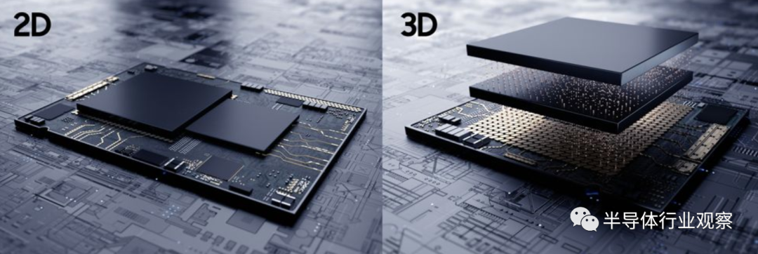
Previously, the chips were all carried out at the 2D level, and the industry research focused on how to increase the number of components per unit area and improve the micro precision. After that, many large factories began to expand their thinking, and applied a stem from Liu Cixin's science fiction piece "three bodies", 3D chips launched a "dimension reduction attack" on traditional 2D chips.
It is also known as the bottleneck of 3D packaging technology, which is beyond the bottleneck of 3D packaging technology.
Compared with traditional packaging, 3D technology can reduce the size and weight by 40-50 times; in terms of speed, 3D technology can save power to make 3D components operate at faster conversion speed per second without increasing energy consumption, reduce parasitic capacitance and inductance, and at the same time, 3D packaging can make more effective use of the effective area of silicon chip. This kind of package has more advantages in integration, performance and power consumption, and has higher design freedom and shorter development time.
It is one of the most promising packaging technologies.
In view of these advantages, the application of advanced packaging technology seems inevitable. According to Myers consulting quoting yole's prediction, the advanced packaging market is expected to grow at a compound annual growth rate of 8% from 2019 to 2024, and the market size will reach US $44 billion by 2024; meanwhile, the compound annual growth rate of traditional packaging market is expected to be only 2.4%. With the increasing demand for artificial intelligence (AI), the demand for semiconductors will increase significantly.
Of course, demand for 3D technology depends on a number of factors, including the booming market for smartphones, tablets, wearable devices and other related consumer goods, and the ecosystem of multiple semiconductor companies (not just a few big ones) committed to upgrading to newer packaging technologies.
At present, there are still uncertainties about 3D Packaging Technology in the market. For example, when and how to adopt these new packaging configurations, and who will dominate the market? All companies in the semiconductor industry (e.g., memory suppliers, logic manufacturers, foundry and packaging subcontractors) must explore strategic alliances and partnerships to ensure the development of viable advanced packaging ecosystems.
For IC manufacturers, foundry and other companies, it is also possible to win over competitors in terms of pricing and quantity. As a result, semiconductor enterprises are faced with crucial decisions in advanced packaging. Whether their goal is to become a pioneer or a fast follower determines the complexity of these choices.
Through the performance of the three major foundry companies in advanced packaging, we may be able to understand one or two.
TSMC's leading position
When it comes to the packaging layout of the wafer plant, TSMC has successively launched 2.5D high-end packaging technology cowos (chip on wafer on substrate) and economical fan-out wafer (integrated fan out) )All of them are very successful. It can be said that from Samsung's share of Apple orders to exclusive Apple orders, Samsung's packaging technology leads its competitors and pushes its industrial position to another peak.
As early as 10 years ago, TSMC has seen that with the rapid miniaturization of semiconductor front-end process, the latter stage packaging technology will not keep up with the pace of the former stage process, and TSMC's forward sprint will be delayed. At that time, Moore's law will really fail, so it resolutely decided to invest in packaging technology, and set up the integrated Department of wire and packaging technology at the end of 2008 Interconnect and Package Development Division, IIPD )。
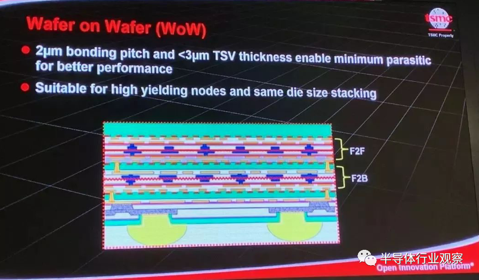
In April 2018, TSMC announced its innovative system integrated single chip (SOIC) multi chip 3D stacking technology for the first time at the 24th Annual Technology Seminar in Santa Clara, California, USA. According to TSMC's explanation at the meeting, SOIC is an innovative multi chip stacking technology and a wafer to wafer bonding technology. SOIC is a new generation of innovative packaging technology based on TSMC's chip on wafer on substrate and multi wafer stacking (wow) packaging technology, which enables TSMC to directly produce 3D IC for customers.
Schematic diagram of TSMC SOIC design architecture.(source:vlsisymposium.org , drawn by CTimes)
At the same time, the wow technology, namely wafer on wafer (wow), is also on display. Just like 3D NAND flash memory multi-layer stacking, the two layers of die are stacked vertically in mirror mode, which is expected to be used to produce GPU for graphics cards and GPU with larger transistor scale.
TSMC said the two packaging technologies will play an important role in the company's advanced packaging layout. In April 19, TSMC announced the completion of the world's first 3D IC package, which is expected to be mass produced in 2021.
In April this year, TSMC announced that the packaging technology was upgraded again. Aiming at the wlsi platform built by advanced packaging technology, tsmc-soic has developed innovative system integrated chip (tsmc-soic) through continuous upgrading of wire interconnection spacing density and system size. In addition to continuing and integrating the existing integrated fanout (info) and on-board chip on wafer (cowos) technologies It provides an opportunity to continue Moore's law, and makes a significant breakthrough in system single chip (SOC) performance.
Tsmc-soic advanced wafer level packaging technology based on 3D IC can integrate multiple small chips into a smaller and thinner SOC. Through this technology, advanced SOC of 7 nm, 5 nm and even 3 nm can be integrated with multi-level and multi-functional chips, and heterogeneous 3D with high speed, high bandwidth, low power consumption, high spacing density and minimum space occupation can be realized IC products.
At present, TSMC has completed tsmc-soic Process Certification, developed micron level bonding pitch process, and obtained extremely high electrical yield and reliability data, which shows that TSMC is ready to produce tsmc-soic for any potential customers.
Recently, Yang Ruilin, research director of the International Institute of Obstetrics, ITRI, pointed out that TSMC has been working in the field of advanced packaging for a long time, so TSMC will be ahead of its competitors in the field of advanced packaging. Foreign investors also expect that advanced packaging will be the key to TSMC building a higher technology and cost threshold and widening the gap with its competitors.
Intel's alternative
At the same time, Intel has also found a new way out in packaging due to the frequent difficulties of 10nm. In December 2018, Intel demonstrated a new 3D packaging technology called "foveros", which is another leap in advanced packaging technology after Intel launched the breakthrough embedded multi chip interconnection bridge (emib) packaging technology in 2018.
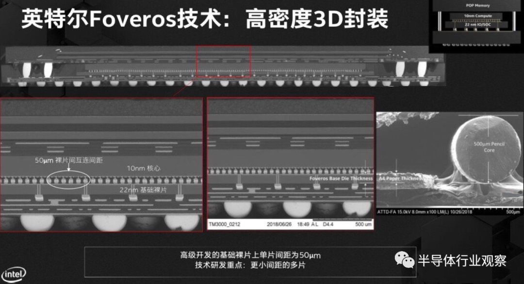
According to reports, this technology is the first time Intel has introduced the advantage of 3D stacking, which can realize the stacking of logic chips on logic chips. Foveros paves the way for integrating devices and systems with high performance, high density and low power consumption. According to Intel, foveros can integrate chips with different processes, structures and uses, so that more computing circuits can be assembled on a single chip to achieve high performance, high density and low power consumption. The "I / O" module of Intel / O can be decomposed into "a variety of chips" and "I / O" modules can be mixed into "new product configurations".
It is reported that Intel will launch a series of products using foveros technology from the second half of 2019. The first foveros product will integrate a high-performance 10 nm computing stack "chipset" and a low-power 22ffl base chip. It will achieve world-class performance and power efficiency in a compact product form.
Recently, in its 2020 architecture day, Intel demonstrated its new progress in the field of 3D packaging technology, which Intel called "hybrid binding" technology.
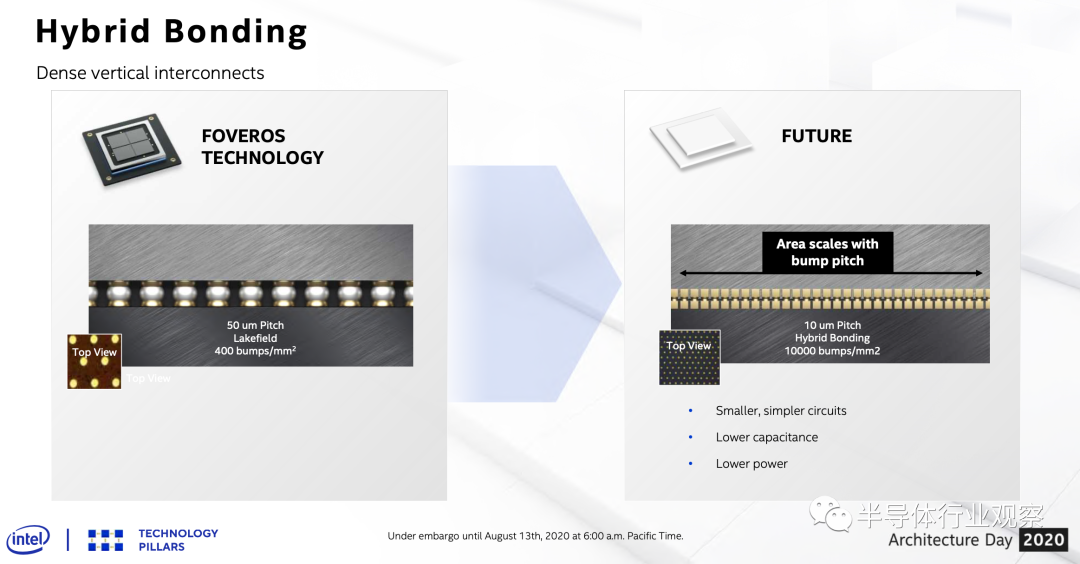
According to Intel's official data, most of today's packaging technologies use the traditional "thermal compression bonding" technology, and hybrid combination is a substitute for this technology. This new technology can accelerate the realization of bump spacing of 10 μ m and below, providing higher interconnection density, bandwidth and lower power.
It has been revealed that test chips using "hybrid bonding" technology have been released in the second quarter of 2020.
In fact, before that, Intel has also tried on 2.5D, which is their emib.
The full name of emib is "embedded multi die interconnect bridge". Because there is no additional silicon intermediate layer, only a silicon bridge is added at the junction of the two bare chip edges, and the I / O pins of the bare chip edge are re customized to meet the bridging standard.
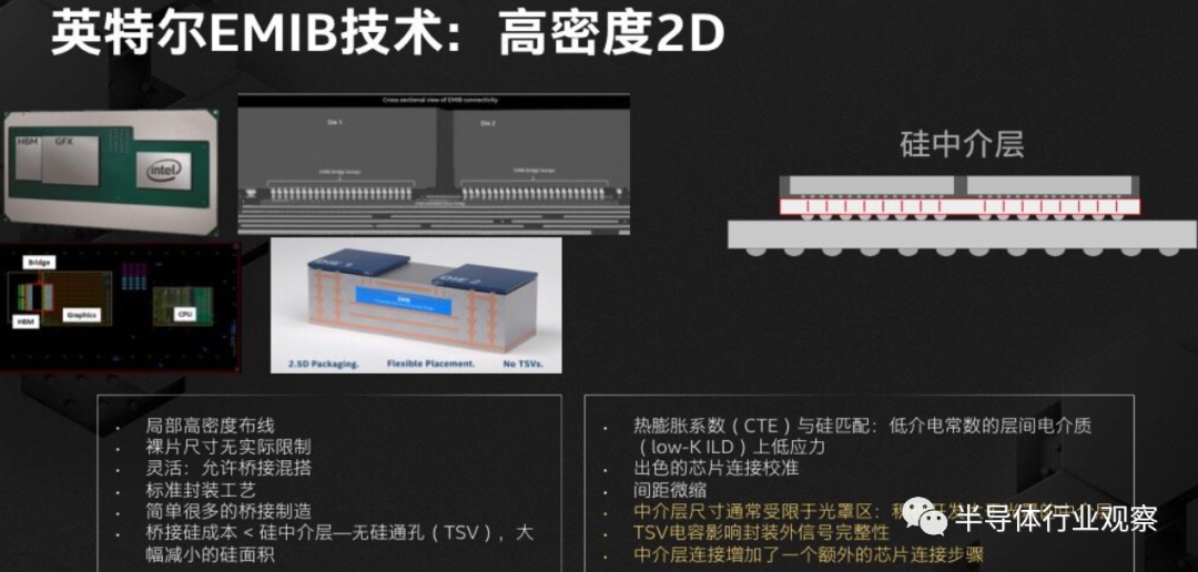
In fanout packaging, Intel is actually a pioneer. In 2009, they launched the ewlb technology and commercial mass production of wafer level fan out packaging. However, the fan-out wafer level package is limited to a narrow application range and is only used for single chip packaging of mobile phone baseband chip. Until 2014, fanout wafer level packaging faced fierce competition from other packaging technologies, which made Intel Mobile give up the technology. So far, Intel has no action on fanout packaging.
Samsung follows suit
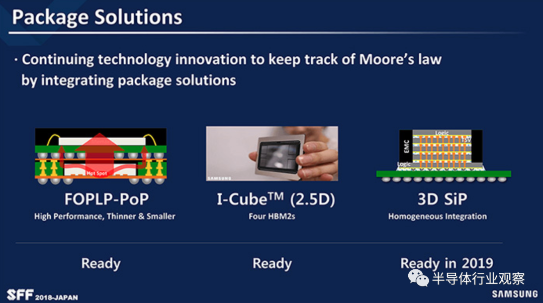
As an old rival of TSMC, Samsung is naturally not willing to be outdone in advanced packaging. For 2.5D package, Samsung has launched the i-cube package process that can compete with TSMC cowos packaging process. At the Samsung wafer foundry forum Japan meeting in 2018, Samsung announced its roadmap in the field of packaging and testing. For 2.5d/3d packaging, Samsung has been able to provide i-cube 2.5D package.
Korean media pointed out that there is no big gap between Samsung and TSMC in terms of technology, while TSMC still has an advantage in packaging technology, but this advantage may be flattened.
Recently, Samsung announced that its new chip packaging technology, x-cube3d, can be put into use. Samsung claims that the technology can make the packaged chip have more powerful performance and higher energy efficiency ratio.
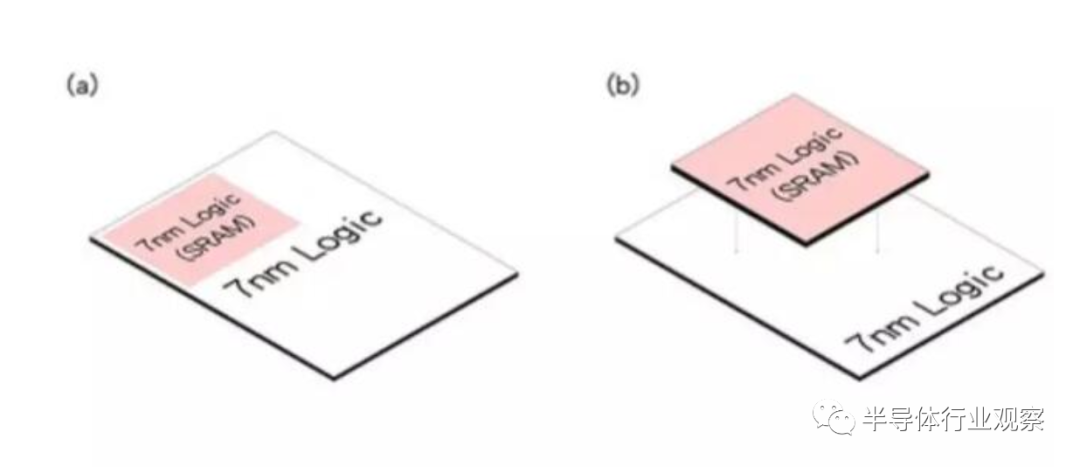
Different from the previous parallel packaging of multiple chips, the new x-cube3d package allows multiple chips to be stacked and packaged, making the structure of the finished chip more compact. The communication between chips uses TSV technology instead of traditional wires. According to Samsung, the technology has been able to stack SRAM memory chips on top of the main chip to make more space for stacking other components. At present, the technology can be used in the product line of 7Nm or 5nm process, which means it is close to large-scale production.
Samsung said TSV technology can significantly reduce the signal path between chips, reduce power consumption and improve the transmission rate. The technology will be applied to the cutting-edge fields of 5g, AI, AR, HPC, mobile chips and VR, which are also places where advanced packaging technology is most needed. As for the development route of chips, Samsung is in line with the major chip manufacturers. It will skip the 4nm process and directly 3nm as the research and development target of the next generation products.
It is understood that the technology will be mainly used in the cutting-edge 5g, AI, AR, HPC, mobile chip and other fields. There is no doubt that the success of Samsung's research and development will certainly enable more users to use 3D packaged chip products, so that more users can enjoy the dividends brought by technological progress.
So far, the three major semiconductor chip manufacturers in the world have 3D or 2.5D packaging technology. The proposal of 3D packaging technology shows that these manufacturers have the same goal by different ways. They are gradually stepping into the same direction of chip development in the future. They are no longer confined to the traditional framework, and pursue more flexible design of different products with stronger performance, richer functions, lower power consumption and more flexible uses.
2019 may be the first year of 3D packaging technology. In that year, both Intel and TSMC have come up with their best weapons to their dominance. By 2020, the war seems to have escalated, and Samsung's participation has added a fire to the war. This year, the three manufacturers are highly concerned about 3D packaging technology, and people in the industry are waiting to see the show of "Top competition".
![]() Tel:0755-83353212
Tel:0755-83353212
![]() Email:4431259@qq.com
Email:4431259@qq.com
COPYRIGHT 2021 JG Technology Co. , Ltd.ICP NO.2020111408